5N Copper Sputtering Target
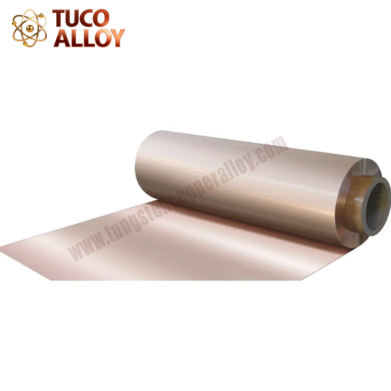
High-purity Copper Sputtering Targets are designed for deposition processes with minimal defect density, optimal grain size, and high-quality surface finish for consistent thin-film formation. Due to their hardness and purity of 99.999% (5N) quality copper, these copper sputtering targets maintain uniform copper film adhesion. The targets are used in copper film deposition in semiconductor, data storage, and optoelectronic industries. This includes reflective and conductive coatings of advanced optics, electroplating, and circuit copper interconnects. In research, copper sputtering targets are used in high-frequency interconnects, thin films for extreme conditions, and novel device architectures. They are used to achieve high uniformity and defect-free coatings for extreme thin-film applications and are used in advanced scientific research and industrial-scale manufacturing. This demonstrates their vast industrial and research value.

Atomic Properties of Pure Copper Targets
| Element | Value |
|---|---|
| Atomic number | 29 |
| Crystal structure | Face-centred cubic |
| Electronic structure | Ar 3d¹⁰ 4s¹ |
| Valences shown | 1, 2 |
| Atomic weight( amu ) | 63.546 |
| Thermal neutron absorption cross-section( Barns ) | 3.8 |
| Photo-electric work function( eV ) | 4.5 |
| Natural isotope distribution( Mass No./% ) | 65/ 30.8 |
| Natural isotope distribution( Mass No./% ) | 63/ 69.2 |
| Atomic radius - Goldschmidt( nm ) | 0.128 |
| Ionisation potential( No./eV ) | 4/ 55.2 |
| Ionisation potential( No./eV ) | 6/ 103 |
| Ionisation potential( No./eV ) | 1/ 7.73 |
| Ionisation potential( No./eV ) | 5/ 79.9 |
| Ionisation potential( No./eV ) | 3/ 36.8 |
| Ionisation potential( No./eV ) | 2/ 20.29 |